Nanotechnology
By Aditya Mittal
May 2005
© MITS Communications – This article is
republished. It was first published in
the June 01, 2005 edition of MITS Communications magazine. For more details on MITS refer to http://www.pilani.com/MITS
Background:
Theoretical Basis:
The laws of classical dynamics begin to deteriorate at
high velocities and small scales where Einstein’s relativity and quantum
mechanics take over, respectively.
Accordingly, small particles traveling at high velocities are subject to
the laws of relativistic-quantum mechanics.
Amazing phenomenon begin to occur in this domain, and new technology is
trying to take advantage of these phenomenon to create miraculous machines.
Nanotechnology
refers to technology at the nanometer (10-9 meters) scale. A nanometer is merely ten angstroms long
where an angstrom is named after Swedish astronomer and physicist, Ångström,
Anders Jonas (1814–1874), who was one of the early formulators of
the science of modern spectroscopy.
Ångström wrote extensively on terrestrial magnetism, the conduction of
heat, and especially spectroscopy. He published a monumental map of the normal
solar spectrum that expressed the length of light waves in units of one
ten-millionth of a millimeter. This unit
of length usually used to specify radiation wavelengths is now known as the
angstrom (10-10 meters). He discovered that hydrogen is present in
the sun's atmosphere, and he was the first to examine the spectrum of the
aurora borealis. Although, the diameter
of atoms varies and the basic unit is taken to be the Bohr radius
(5.2917725 x 10⁻¹¹ m), the diameter of an atom
depending upon the element is approximately one to five angstroms. This puts from 2 to 10 atoms in a nanometer
and 2000 to 10000 atoms in a micrometer.
For example, there are about 3 silicon atom diameters in a nanometer.
Quantum
Mechanics becomes extremely important at these atomic scales. Quantum Mechanical uncertainty begins to play
a large role in our ability to determine how a nanoscale machine such as a
small robotic arm will behave in certain conditions. Effects like electrons tunneling through
potential barriers can form both hindrances and advantages in creating such
machines. Interestingly, the scanning
tunneling microscope (STM) widely used in both industrial and fundamental
research to obtain atomic-scale images of metal surfaces, itself uses the
quantum tunneling effect to view and manipulate nanoscale particles, atoms and
small molecules and to map surfaces. The STM, first used in the mid-1980s,
allowed scientists not only to see details of atomic structures, but also to
manipulate those structures.
Unlike relativity, which has remained unchanged since
Einstein’s formulation, quantum mechanics is still being formulated to some
extent. This theory is not a result of
only one person but of many people’s calculations and ongoing experiments. Alongside, other theories are also developing
for describing small scale and high velocity behaviors such as Superstrings
which has been quite popular in the recent years. The theoretical developments are closely
correlated with recent discoveries in nanotechnology that remained unexplained
by older theories. The seemingly sudden
new discoveries are not a result of an impulsive idea but sequences of small
experiments gradually done in labs until a refined product is seen. When the new discovery comes into the
attention of thousands of physicists all of a sudden, new ideas begin to
evolve, and new theories and experiments are formed. Take for example, quantum dots which are
still undergoing this gradual development.
Quantum
dots are tiny particles of semiconductors such as
cadmium selenide that behave as if they were individual atoms. They can absorb light energy, kicking their
internal electrons up to higher energy levels, and then release the energy by
emitting light. A quantum dot fluoresces much more brightly than a dye
molecule, making it a desirable marker especially to track the moving molecules
of a living organism since an electron microscope cannot be used. This process is known as biological tagging. Now in
2004, The University at
Also, in May 2005, Researchers
at the U.S. Department of Energy's National Renewable Energy Laboratory showed
that the materials used to create quantum dots can also be used to greatly
improve solar cell electricity production because quantum dots can furnish as
many as three electrons from one high energy photon of sunlight. When today's
photovoltaic solar cells absorb a photon of sunlight, the energy gets converted
to at most one electron, and the rest is lost as heat. Today’s best cells convert only about
33 percent of the sun's energy into electricity. However, NREL and NRL (Naval Research Lab in
Vision of Nanotechnology:
People have wanted
to be rich for centuries. People have
been trying to create gold ever since gold became the measure of wealth. People have also been trying to make diamonds
because not only are they expensive and a display of aristocracy, but also
rare, and quite useful in industrial applications such as cutting. Unlike gold, diamonds are constructed of
carbon which is readily available at dirt cheap prices. If anyone could cheaply put carbon atoms
together to form diamonds, he would become rich instantly. Dr. Ralph Merkle sees atoms as LEGO blocks. “Today’s manufacturing methods are very crude at the molecular
level. Casting, grinding, milling and even lithography move atoms in great
thundering statistical herds. It's like trying to make things out of LEGO
blocks with boxing gloves on your hands. Yes, you can push the LEGO blocks into
great heaps and pile them up, but you can't really snap them together the way
you'd like.
“In the future, nanotechnology
will let us take off the boxing gloves. We'll be able to snap together the
fundamental building blocks of nature easily, inexpensively and in most of the
ways permitted by the laws of physics. This will be essential if we are to
continue the revolution in computer hardware beyond about the next decade, and
will also let us fabricate an entire new generation of products that are
cleaner, stronger, lighter, and more precise.”
In
Aditya Mittal’s science fiction book Fierce Game of Foolish Geniuses: The
Opening of Chess a futuristic robotic society is envisioned in which a
printer would be able to print not only on paper by putting atoms of ink on it,
but to put individual atoms together in any 3D configuration. In other words, a printer would be able to
print a diamond given carbon atoms or even a potato if someone was hungry. In this robotic society, elements came
through pipelines into a home or office just the way data comes in bits through
an internet coaxial cable today. Of
course, these elements were paid for by the user to the provider.

Some
time back, there was an article in Science
News envisioning an elevator to space – that is from ground to a space
station in space. This elevator would be
pulled up and down by carbon nanotubes which were claimed to have enough
strength to hold up such a system. A
simple google search for ‘space elevator’ will result in much more information
on this subject.
In
Michael Crichton’s novel Prey, there was a nanotechnological black swarm
of predator robots. This was built on
the swarm model developed in
Ideas, Experiments and Research:
Molecular manufacturing
Molecular manufacturing is the
envisioned construction of molecules one atom at a time, where any structure
consistent with physical laws can be made at costs not exceeding the cost of
the required raw materials and energy.
This idea was directly seen in my printer vision. For more detailed analysis of the subject see
Merkle’s articles “Molecular
Manufacturing: Adding Positional Control to Chemical Synthesis”
published in Chemical Design Automation News, Volume 8, Numbers 9 &
10, September/October 1993, page 1 and “Convergent Assembly” published in Nanotechnology
8, No. 1, March 1997, pages 18-22.
This material is not as recent as the topics discussed here, however, is
crucial to understanding the basic details of molecular manufacturing.
Assembly
The current idea of assembling an object from
nanoparticles consists of using robotic arm(s) to move particles into the right
positions. We wish to assemble in both
serial and parallel as if there are many assembly lines. Exponential assembly, convergent assembly,
and self-replication are key ideas in such an assembly. According to the people at Zyvex who are
developing huge numbers of miniature robotic arms exponential assembly is “a manufacturing architecture starting with a single tiny
robotic arm on a surface. This first robotic arm makes a second robotic arm on
a facing surface by picking up miniature parts — carefully laid out in advance
in exactly the right locations so the tiny robotic arm can find them — and
assembling them.” These robotic arms are
a part of MEMS (Micro Electro Mechanical System). Convergent assembly on the other hand is the
idea that small parts can be assembled into large parts, which can be assembled
into still larger parts, and so forth.
Finally, self-replication is the idea that a particle can create more of
itself, given the components to make it in the right positions. The idea of self-replication is built into
the idea of exponential assembly as defined by Zyvex.
Carbon Nanotubes
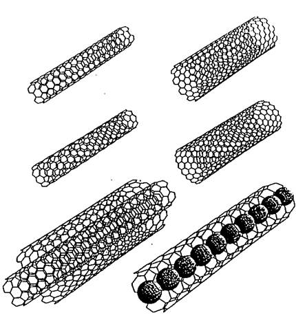
The above image shows examples of carbon nanotube
structures, including multiwalled and metal-atom-filled nanotubes. Image taken from http://www.wtec.org/loyola/nano/04_03.htm
on May 27, 2005.
As mentioned earlier, the ability to make diamonds
cheaply is desired; therefore, in the recent years much emphasis has been given
to constructing compact stable structures out of carbon atoms. 1996 Nobel Prize laureates Robert F. Curl,
Harold W. Kroto, and Richard E.
Smalley discovered the carbon structure Buckminsterfullerene, more commonly
known as the "buckyball" consisting of 60 carbon atoms arranged like
a ball. In the years that followed a
common device for holding carbon structures became seamlessly wrapping
graphitic structures around cylinders.
This technique has also been applied to other elements but carbon
remains most popular. These structures
could be made anywhere from just a few nanometers in cylindrical diameter up to
a millimeter in diameter. This allows
for multifarious length-to-width aspect ratios.
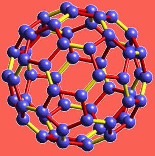
Buckyball
The
following passage from “The Space Elevator Comes Closer to Reality” by David
Leonard shows us not only the strength and fast pace research of these carbon
nanotubes, but also how much is expected:
The hurdle to date,
Edwards said, has been the commercial fabrication of carbon nanotubes. Both
Given the far stronger-than-steel ribbon of carbon nanotubes, a
space elevator could be up within a decade. "There's no real serious
stumbling block to this," Edwards explained.
"The making of carbon nanotubes is moving very quickly,"
said Hayam Benaroya, a professor in the Department of Mechanical and Aerospace
Engineering at Rutgers in
"Perhaps within our lifetimes we might actually see real
designs of skyhooks and space tethers, these kinds of things. They may be
feasible at reasonable cost," Benaroya said.
If things really do move at the pace expected by this
article it would not be long before we will really be creating diamonds. Today, many firms are patenting various
designs of these nanotubes such as “buckytubes” which are small diameter carbon
nanotubes on which Carbon Nanotechnologies, Inc (CNI)
reached 30 patents this year.
Designs not only vary the diameter of the tube but also the number of
layers around the cylinder.
Following is the quantitative
measure of some carbon nanotube properties from Discover Magazine, January 1999, page 38:
Superstrong Materials: Embedded into a composite, nanotubes have enormous
resilience and tensile strength and could be used to make cars that bounce in a
wreck or buildings that sway rather than cracking in an earthquake.
Tensile Strength: 45 billion Pascal vs. 2 billion Pascal for the best steel alloys before they break
Density & Lightness: 1.33 to 1.40 grams per cubic centimeter vs. 2.7 g/cm^3 for aluminum (& 8.0 g/cm^3
for steel)
Resilience/Memory: Can be bent at large angles and re-straightened without damage. Carbon fibers
and normal metals fracture at grain boundaries (causing wrinkles, creases,
dents, and breakage).
Heat Transmission: Predicted to be as high as 6000 watts
per meter per Kelvin at room temperature vs. 3320 W/m/K for nearly pure diamond
or 430 W/m/K for silver. (Nanotubes have highest known heat transmission)
Temperature Stability: Stable up to 2800 deg. Celsius (5000 deg. Fahrenheit) in a vacuum; 750 deg C in air (1400 F);
Size:
0.6 to 1.8 nanometers in diameter (Threads of nanotube fibers could be woven
into a cloth or fabric.)
Electrical Properties: Can be varied from semiconducting to highly conducting;
semiconductor material could be dull in color while highly conducting material
could appear shiny and metallic.
Following is from Scientific American, January 2000:
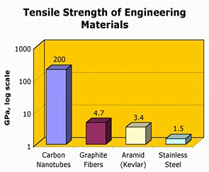
Clearly,
the numbers are different. Searching
different sources we find that carbon nanotubes are about six or more times
lighter than steel and 10 to 100 times stronger than steel depending upon the
type of steel and carbon nanotube and exact details of measurement. But clearly, nanotubes win by a significant
amount.
Photonics and Electronics
Short range fiber optics has been low-profile for the
past few years while electronics has been gaining because of its ability to
produce results cheaply. Fiber optics
has been an expensive process of constructing tube like structures made of
glass or plastic to carry photons that carry data. Due to high costs of fiber production, it is
only used for large amounts of data transmission over long distances to
minimize costs. It works well over long
distances because photons are fast and the energy loss from the fiber is
minimal. Along with this, optical fiber
amplifiers can be used to restore the lost energy along the way. For imagination purposes, it is useful to realize
that a single optical fiber can carry as many as 300,000 telephone calls.
However, speeding techniques in electronics are moving towards exhaustion as
electrons can only travel so fast through circuitry and we can only make the
circuit small enough. As things move
along, we might very well be forced to supplant our electronics with photonics
– that is transmitting photons through the wires instead of electrons. It has been estimated that a photonic
internet could be carrying 160 gigabits per second.
“If the promise of photonic
technology is realized, the high-speed processing and movement of data today
will seem so sludgelike, people of the future will wonder how we ever got
anything done. Photonic technology is still a long way down the road but the
goal is a few steps closer now.” – A
Few Steps Closer to Nanoscale Photonic Technology by U.S. Department of Energy’s Lawrence Berkeley National
Laboratory (Berkeley Lab)
Scientists working with the Berkeley Lab and
At
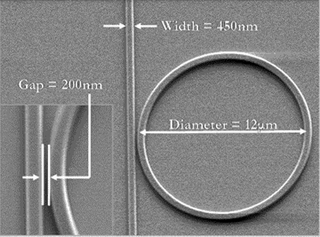
Image Copyright ©
Cornell University
The
development of photonics will still take some time. We still need to explore the nanotechnology
door before jumping into the photonics.
The systems that build the field of photonics might very well be
constructed of nanotubes and other nanoscale structures. More theoretical advancement may also be
needed before photonics is really applied.
We started with discussing relativistic quantum mechanics but up until
now we have only really dealt with quantum mechanics. That is behavior at the small scale limit,
namely, the atomic scales at which we have needed to understand the behavior of
electrons. However, for photons in small
structures both quantum mechanics and also relativity will be important when
determining time delays for various components.
Due to more tedious timing calculations it might become more convenient
to design asynchronous self-contained circuits rather than using system clocks
as with present day computers.
The Labs and Companies:
Iomega – recently got U.S. Patent No. 6,879,556 titled Method and Apparatus for
Optical Data Storage which is a nano-technology-based subwavelength optical
data storage technology called AO-DVD (Articulated Optical - Digital Versatile
Disc). In the future this technology is
expected to lead to 40-100 times better DVD’s.
This invention is a recent winner of Nanotech Briefs' Nano 50 awards which
began this year. On June 7-8, 2005 a
Nano2005 conference is being held at The Westin,

Because it will be
exhaustive to continue to write about the hundreds of labs and companies
rapidly discovering the field following is a list of some
|
3i |
Massachusetts Technology Collaborative |
Journals and References:
Technology
Review: MIT's Magazine of Innovation – MIT Tech Review is a monthly science magazine
that covers a variety of topics currently in research including
nanotechnology. Its cover price is
$59.88 per year.
IEEE Transactions On
Nanotechnology - The scope of the
IEEE Transactions on Nanotechnology will include the physical basis and engineering
applications of phenomena at the nanoscale level across all areas of science
and engineering. It is
a quarterly magazine and the price is $549.63 per year.
Journal Of Nanoscience And Nanotechnology
– A monthly magazine that consolidates research activities in nanoscience and
nanotechnology into a single, and unique reference source. Articles cover
synthesis of nanostructures, atomic characterization, bioassemblies,
nanoprobes, quantum factors and more. The price for
a year’s subscription is $530.82.
International Journal Of Nanotechnology - The journal includes original articles on all subjects and
topics related to nanotechnology, along with review papers, conference reports,
essays, notes, news, and comments.
This is a quarterly journal at $474.07 per year.
Nanotechnology Law &
Business – Quarterly magazine at $256.55 per year.
Nanotechnology – Monthly magazine aimed at
promoting the dissemination of research and improving understanding amongst the
engineering, fabrication, optics, electronics, materials science, biological
and medical communities. Yearly price
is $480.11.
Journal Of Biomedical
Nanotechnology – Quarterly journal priced at $272.07 per year.
Nanomedicine :
Nanotechnology Biology And Medicine – Quarterly journal priced at $84.74 per
year.
- http://www.rootburn.com/portfolio/nano/
- a very nice presentation of nanotechnology basics – a must read for the
audience who enjoyed this article
- http://www.nanodynamics.com
– website of NanoDynamics, Inc.
which is a manufacturer of
nanomaterials
- http://www.nanotechbriefs.com/
– a new online nanotechnology and MEMS magazine
- http://www.physorg.com
– a great site for physics and technology news with many great
nanotechnology articles that are very up to date
- http://www.zyvex.com/nano/
- concepts of molecular nanotechnology and lots of links
- http://www.pa.msu.edu/cmp/csc/nanotube.html
- See this website for lots of links to nanotechnology sites, past and
future events, nanotechnology products and so forth.
- http://www.cnanotech.com/pages/resources_and_news/3-4_newspress_releases.html
- website of Carbon Nanotechnologies Inc